Time:2023/04/27
Author:from SEMI
The SEMI Compound Semiconductor Materials Technology Forum, hosted by SEMI China and hosted and sponsored by Guangdong Zhongtu Semiconductor Technology Co., Ltd., was held on April 27, 2023 in We Valley, Dongguan, Guangdong.
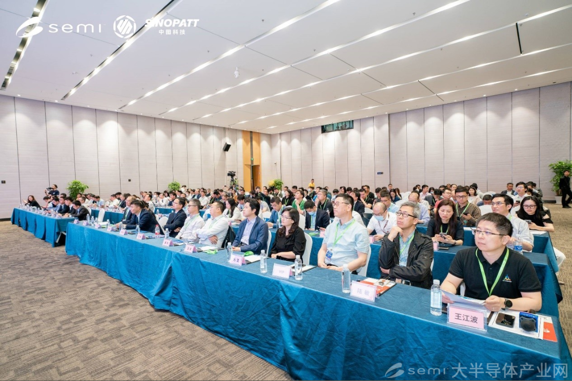
The rapid rise of new semiconductor materials represented by compound semiconductors has broad application prospects in fields such as new energy vehicles and consumer electronics. The market space for compound semiconductors represented by gallium arsenide (GaAs), gallium nitride (GaN), and silicon carbide (SiC) continues to expand. With strong downstream demand for compound semiconductors, the prospects are bright and promising.
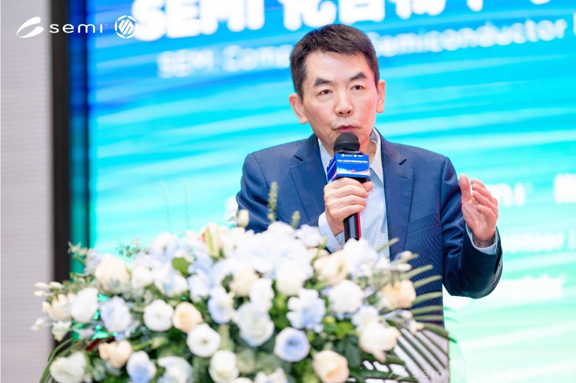
Mr. Ju Long, Global Vice President of SEMI and President of China, attended the meeting and delivered an on-site speech. President Ju extended his welcome to the guests attending this meeting, and shared with you the recent situation and prospects of the Semiconductor industry. Last year, the global semiconductor industry grew by 3.2% to reach a market size of 573.5 billion US dollars. This year, the president described the current Semiconductor industry as "the cold wave will wait for the spring, and the long wind and waves will sometimes break". Since the third quarter of last year, the Semiconductor industry has entered a downward cycle due to sluggish growth of the terminal consumer electronics market, intensified geopolitical, and the world's macroeconomic and political situation. According to the latest data of the current first quarter, the industry sales generally declined, and the inventory was more serious than expected at the beginning of the year. It is estimated that the Semiconductor industry will start to recover in the fourth quarter of this year or early next year. In the downward cycle of the industry, the automotive Semiconductor industry is the best, especially in China's Alternative fuel vehicle market, which has the fastest growth rate. Many power and compound semiconductor companies present are related to the automotive industry. In the face of the current severe international situation and various uncertainties, Julong put forward his view on the way forward for China's Semiconductor industry: market is the king, innovation is the right way, and talent is the top way.
Finally, Mr. Ju would like to express his gratitude to the organizers and the leaders present. We also welcome everyone to participate in the SEMICON China 2023 held in Shanghai from June 29th to July 7th.
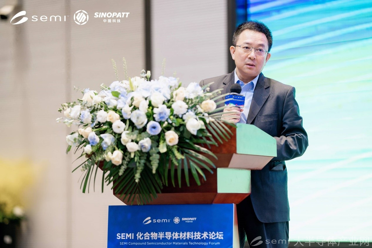
Liu Wei, Deputy Secretary of the Dongguan Municipal Party Committee and Secretary of the Songshan Lake Party Working Committee, said in his speech that a new round of scientific and technological revolution and industrial reform are going deep into development. Compound semiconductor is the "most important tool of the country", an important content and key support to promote scientific and technological self-reliance and high-quality industrial development. He sincerely hoped that entrepreneurs and experts would strengthen exchanges and cooperation, together ignite the "core" fire with innovation, and make greater contributions to promoting the development of the Semiconductor industry!
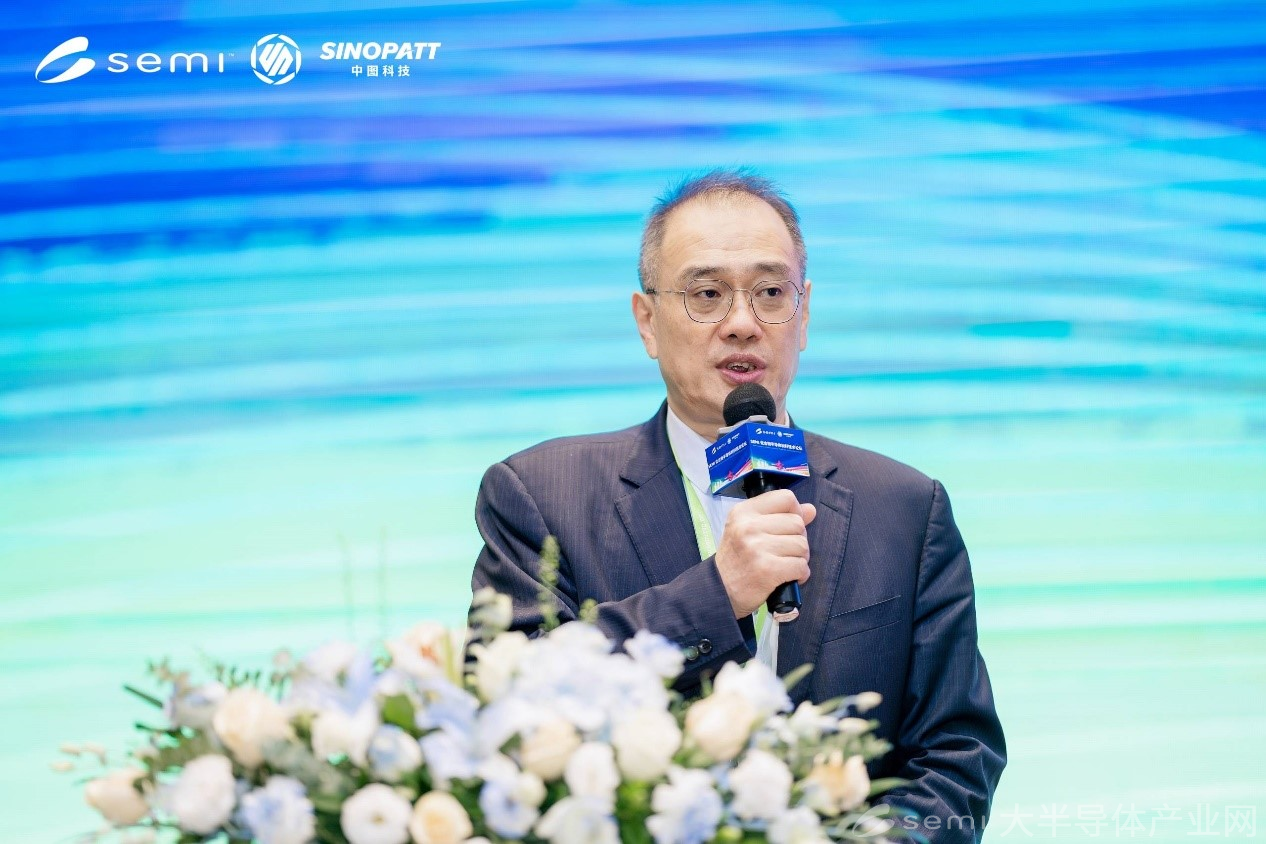
Kang Kai, Chairman and General Manager of Guangdong Zhongtu Semiconductor Technology Co., Ltd., stated in his speech that as a local enterprise in Dongguan, Zhongtu Technology has been registered and developed in Songshan Lake, and has become one of the global leaders in GaN based LED graphic substrates. President Kang also said that today's gathering of forum elites gave a good opportunity to exchange and learn the application of compound semiconductor materials and technological development, and wished China's Semiconductor industry continuous development and progress.

The morning session of the meeting was presided over by Mr. Wang Jiangbo, Vice President of Huacan Optoelectronics Co., Ltd., and the afternoon session was presided over by Mr. Lu Min, General Manager of Changzhou Zhenjing. Experts from Huacan Optoelectronics, Zhongtu Semiconductor, Suzhou Hanhua Semiconductor, Oti Optoelectronics, Songshan Lake Materials Laboratory, Cosi Information, Guangdong Pioneer, Beijing Mingga Semiconductor, Gate Semiconductor, Shanxi Shuoke, Shenzhen Zhongji New Materials, and Chem Semiconductor participated in this forum and shared their reports. Nearly 260 guests from the industry attended this meeting.

Wang Jiangbo, Vice President and Chief Technology Officer of Huacan Optoelectronics Co., Ltd
Wang Jiangbo, Vice President and Chief Technology Officer of Huacan Optoelectronics Co., Ltd., elaborated on the research and prospects of the new generation of Mini/Micro LED chip technology for display. Dr. Wang mentioned that as a leading domestic Mini/Micro LED chip enterprise, Huacan Optoelectronics has launched multiple terminal products in the Mini LED market, and key progress has been made in the cooperation between Micro LED products and strategic customers. Dr. Wang Jiangbo pointed out that small screen wearable devices and high-end display applications with large screens will be the main entry points for opening up Micro LED applications. Huacan Optoelectronics Micro LED small and medium-sized products continue to be supplied in small batches, and the yield of large-sized wafers has further improved; Micro LED pixel devices achieve on-screen illumination and are expected to be mass-produced on a small scale by 2023; The micro display screen used for AR close eye display has achieved dynamic display of multi-color sample screens. The company has transferred a large amount of technology and jointly developed with equipment manufacturers, resulting in continuous improvement in yield and smooth progress.
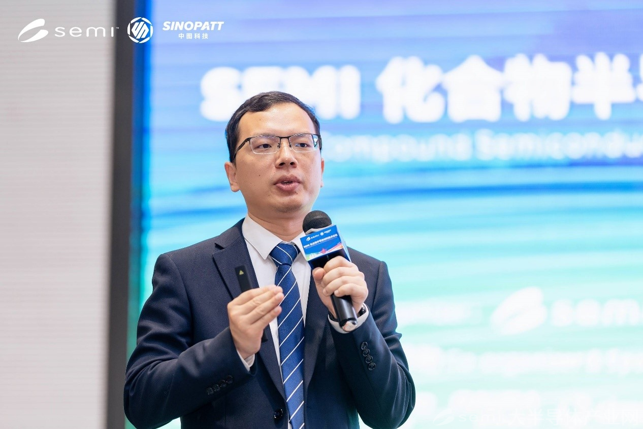
Zhang Neng, Product Director of Guangdong Zhongtu Semiconductor Technology Co., Ltd
Zhang Neng, Product Director of Guangdong Zhongtu Semiconductor Technology Co., Ltd., explained the application and development trend of sapphire graphical products to everyone. Mr. Zhang introduced that sapphire material, as the most widely used substrate for the third generation semiconductor GaN, can improve the quality of epitaxial crystals, improve light extraction rate, and adjust light intensity distribution through graphical effects. At present, it is not only applied in multiple traditional LED fields, but also rapidly developing in different application scenarios such as Mini/Micro LED new displays, UVC, automotive lighting, and power electronic devices. Based on the design and process control capabilities of different graphic structures, Zhongtu Technology can provide PSS and MMS products that achieve various application indicators, better serving the needs of end customers.

Fan Qian, Vice President of Suzhou Hanhua Semiconductor Co., Ltd
Fan Qian, Vice President of Suzhou Hanhua Semiconductor Co., Ltd., shared the application and prospects of 3DIC technology in the field of compound semiconductor devices. He talked about the advantages and challenges of 3DIC technology in the field of devices, and the key technology process of 3DIC - Hybrid bonding at room temperature hybrid integration, which brings new changes to the display field. In the future, Hanhua will live up to expectations, continuously research and innovate, and deeply empower the high-end display application industry chain.
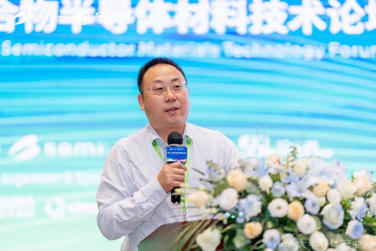
Wu Liang, CEO of Oti Optoelectronics Technology (Hangzhou) Co., Ltd
Wu Liang, CEO of Oti Optoelectronics Technology (Hangzhou) Co., Ltd., discussed in detail the latest progress and challenges in the growth of large-sized and high-quality aluminum nitride single crystal PVT. Mr. Wu elaborated on the enormous potential of AlN in deep ultraviolet optoelectronics, laser and sensor equipment, as well as power equipment and fast electroacoustic SAW/BAW equipment. The high cost of AlN substrates mainly comes from the technical difficulties of crystal growth, such as impurity removal, extremely high temperature processes, consumables costs, iterative growth to expand size, and low yield.
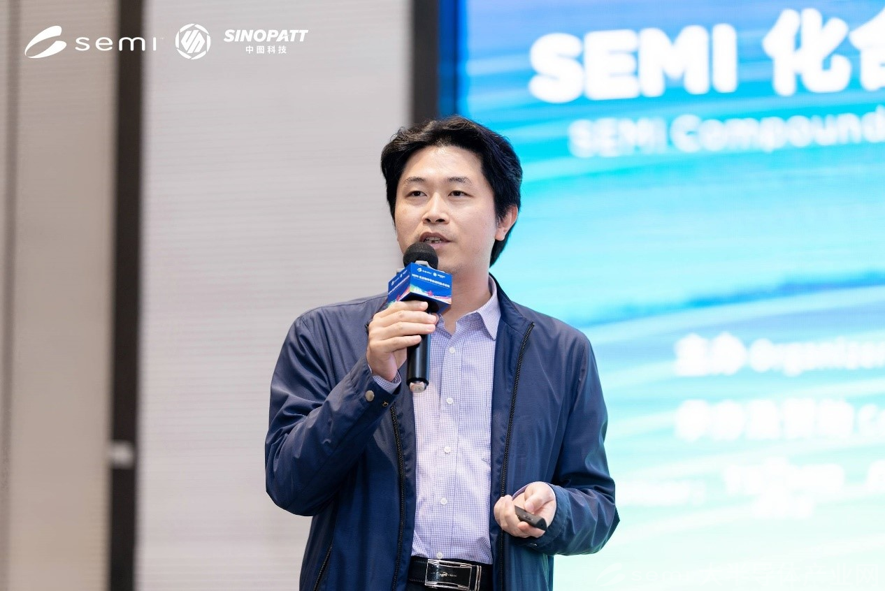
Wang Yang, Deputy Director of Microprocessing and Device Platform at Songshan Lake Materials Laboratory, Researcher level Senior Engineer
Wang Yang, Deputy Director of Microprocessing and Device Platform at Songshan Lake Materials Laboratory and Researcher level Senior Engineer, discussed in detail the development of compound semiconductor materials and device micro/nano processing platforms. The Microprocessing and Device Platform is a sub platform under the public technology platform of Songshan Lake Materials Laboratory. Based on the forefront of micro and nano processing technology and the development trend of the semiconductor device industry, the platform actively lays out advanced microelectronic devices, optoelectronic devices, MEMS&NEMS devices, flexible devices, 3D hybrid integrated devices, and other fields to meet the needs of electronic information, advanced displays, artificial intelligence, clean energy The development of new concept materials processing and other technologies demands micro and nano processing.
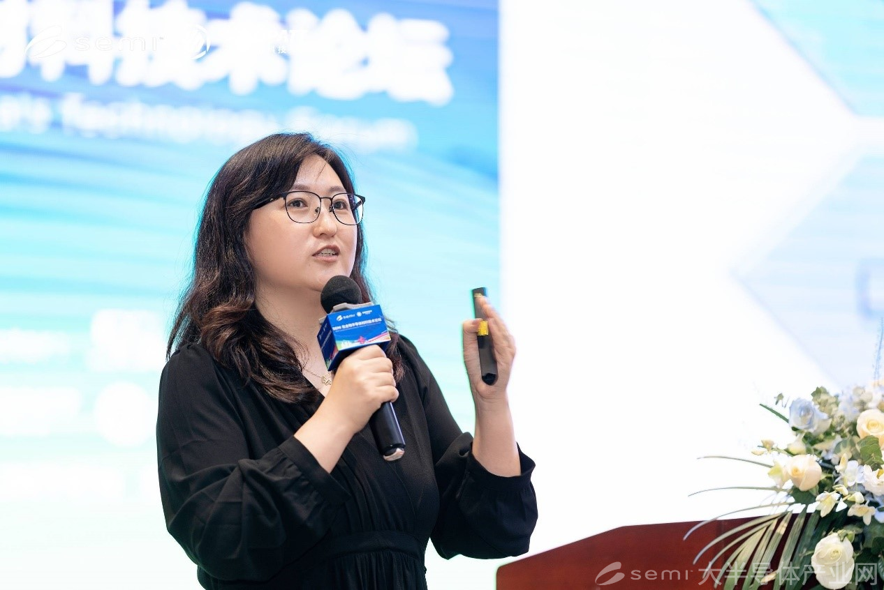
Executive Vice President of Kesi Information Technology (Shanghai) Co., Ltd
Liu Bo
Liu Bo, executive vice president of Cosilicon Information Technology (Shanghai) Co., Ltd., introduced the exploration of intelligent manufacturing in compound Semiconductor industry. Ms. Liu Bo elaborated that compound Semiconductor industry is a strategic emerging industry that is at the international leading level in China. The automation and intelligence of the production process require us to actively develop and implement equipment level standards, strive to improve productivity and reduce operating costs, and accelerate the transition to intelligent manufacturing. Standard communication interfaces and device data are the basis of Big data and artificial intelligence. The SECS GEM standard has been widely used globally for over twenty years and is a mature and validated series of standards. Some compound semiconductor equipment manufacturers have experience in semiconductor front-end and back-end equipment, and the equipment can provide corresponding SECS GEM interfaces.
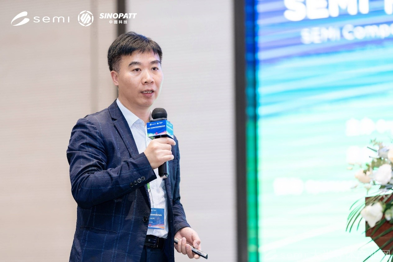
Zhou Tiejun, General Manager of Guangdong Pioneer Microelectronics Technology Co., Ltd
Zhou Tiejun, General Manager of Guangdong Pioneer Microelectronics Technology Co., Ltd., shared the prospects for the processing and application of large-sized compound semiconductors. Mr. Zhou introduced the stable mass production and supply of 6 "GaAs and 4" InP crystal growth and wafer processing on the supply side of substrate materials, which have achieved large-scale production and supply. 6 "GaAs have formed large-scale device mass production in the fields of 3D sensing and laser applications, such as VCSEL for 3D sensing and digital communication, and edge emission (EEL) devices for industry, aerospace, and national defense. 4 "InP has also achieved large-scale production of optical communication application modules.
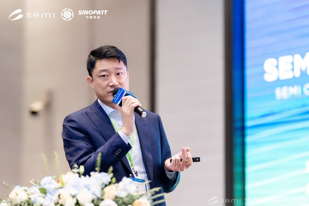
Chen Zhengwei, General Manager of Beijing Mingjia Semiconductor Co., Ltd
Chen Zhengwei, general manager of Beijing Mingga Semiconductor Co., Ltd., discussed in detail the industrialization of ultra wide band gap semiconductor material Gallium(III) oxide and its devices. Dr. Chen introduced that Gallium(III) oxide Ga2O3 is the fourth generation of wide band gap semiconductor material after Si, SiC and GaN β- Power devices based on Ga2O3 single crystal have higher breakdown voltage and lower conduction resistance, resulting in lower conduction loss and higher power conversion efficiency. They have great application potential in power electronic devices. Beijing Mingga Semiconductor Co., Ltd. is committed to R&D and production of artificial crystal materials, including the fourth generation semiconductor materials Gallium(III) oxide, high-frequency Indium phosphide crystals and large-scale doped optical crystals.

Scientist of Gallate Semiconductor Technology (Shanghai) Co., Ltd Liu Deang
Liu Deang, a scientist at GaTe Semiconductor Technology (Shanghai) Co., Ltd., elaborated on the HVPE growth technology for 4-inch gallium nitride self-supporting wafers. Dr. Liu introduced that the application of wide bandgap semiconductor GaN materials is limited due to the lack of homogeneous epitaxial substrate gallium nitride self-supporting wafers. HVPE technology can achieve the commercialization of GaN self-supporting wafers, but currently most can only achieve 2-inch growth. By properly designing the growth cavity to ensure the uniformity of the flow field temperature field, combining self stripping technology and lateral epitaxial technology to control stress and dislocation density, the growth of 4-inch GaN self-supporting wafers has been achieved.

General Manager Assistant/Senior Engineer Ma Kangfu of Shanxi Shuoke Crystal Co., Ltd
Ma Kangfu, Assistant General Manager of Shanxi Shuoko Crystal Co., Ltd., discussed in detail the analysis and application prospects of SiC single crystal growth technology. Mr. Ma first introduced the physical properties of SiC materials and compared them with traditional first generation semiconductor Si materials, analyzing the advantages of SiC over Si materials. Subsequently, the application scenarios and market scale of semi insulated SiC and N-type SiC were elaborated separately. Subsequently, the defects and growth technology of SiC single crystal were analyzed, and the development plan and research progress of our unit were briefly introduced. Finally, suggestions were made for the development of the industry.
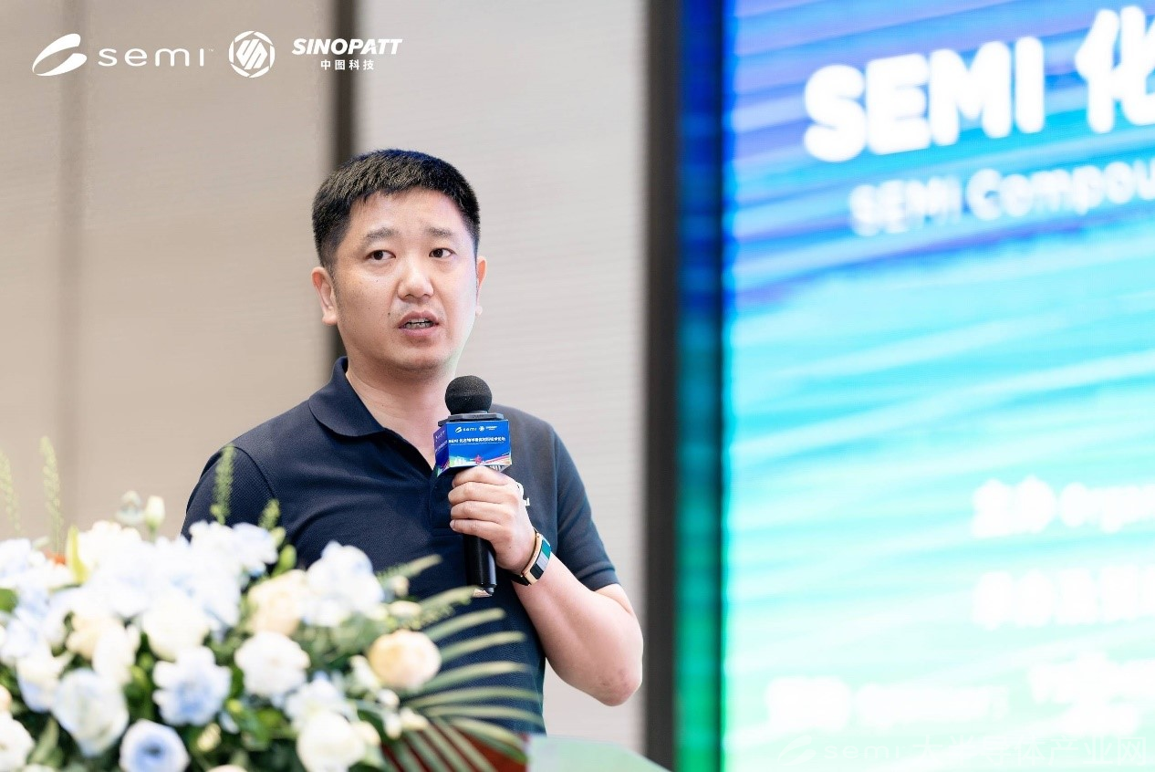
Chen Bin, Founder/Chairman of Shenzhen Zhongji New Materials Co., Ltd
Chen Bin, founder/chairman of Shenzhen Zhongji New Materials Co., Ltd., discussed in detail the latest progress and development trends of SiC substrate cutting, grinding and polishing technology. Mr. Chen introduced the market development trend of silicon carbide: with the expansion of new energy vehicles, photovoltaic energy storage and other fields, the demand has increased. The proportion of cutting, grinding and polishing costs is high, and traditional process equipment investment is large. Shortening the processing process, optimizing the process, and improving yield are the directions for the development of processing technology.
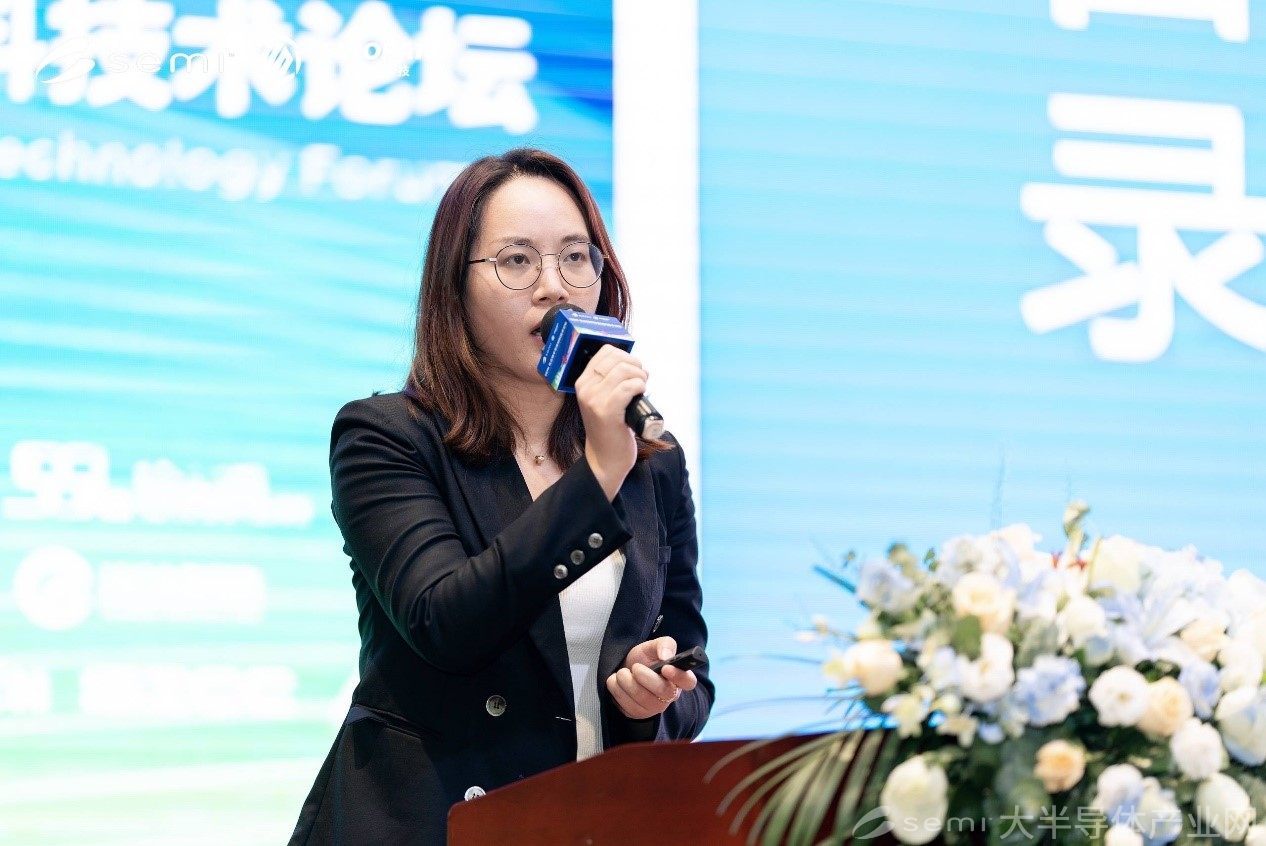
Zhang Xing, CEO of Huahe Jidian (Xiamen) Semiconductor Technology Co., Ltd
Zhang Xing, co-founder and CEO of Huahe Jidian (Xiamen) Semiconductor Technology Co., Ltd., shared the latest progress in the industrialization of wafer level and heat sink level diamonds. Diamonds have excellent characteristics such as high thermal conductivity, high breakdown electric field, high carrier mobility, high carrier saturation rate, and low dielectric constant. Huahe Jidian is based on internationally leading diamond innovation research and development capabilities and large-scale production capabilities, We provide diamond heat sinks and wafer grade diamonds as heat sink materials or substrate materials for our customers, effectively solving the heat dissipation problem of high-frequency and high-power chips or devices.
The 2023 Spring Meeting of the SEMI Compound Semiconductor Standards and Technology Committee and the SEMI Compound Semiconductor Materials Technology Forum have successfully concluded. SEMI warmly welcomes industry experts to participate in the SEMICON Exhibition from June 30 to July 1, as well as the Power and Compound Semiconductor International Industry Forum and the Power and Compound Semiconductor Automotive Application Development Summit Forum.
——from SEMI